
Updated 26th September 2020
Over the past years I have had some health issues, my wife has major health issues, we moved house and I lost both workshop and hamradio facilities. I was forced to "downsize", which in reality means getting rid of stuff to which you have become attached during your life.
About 7 years ago I sold all the really good stuff, such as a HP spectrum analyser, with tracking generator, dual-beam oscilloscope, RF generators, AF generators - the lot. That is something I really regret. So now I am building some basic equipment (but smaller) so that I can continue my hobby within a limited space. Today's project is an Analogue Audio Frequency (AF) signal generator.
Since I have no workshop facilities until later in the month, I am just sitting here in Spain, designing and drawing the prototype PCBs. Today's project I am pretty sure to 99% it works fine. I built this project about 30 years ago when more suitable components were available. I have made a few additions and changes to take into account the components that are available today. I will also give you the info on the changes, so if you intend to build it then you can better correct any possible error.
Since writing this I have built the prototype and it works exactly as predicted. No-longer a theoretical project. No component changes. I love LT-Spice.
The basic circuit is a single Operational Amplifier (OpAmp) used in a Wein Bridge oscillator circuit. The OpAmp oscillator used the non-inverting input to the amplifier, but a series RC circuit (C2/R2) gives a phase change between amplifier output and input. A second RC (C1/R1) is a parallel combination which shunts the feedback signal. Since both resistance and capacitance is used, the two circuits are frequency dependant.
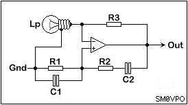
Because the OpAmp is non-inverting, the feedback must be in phase with the output to get oscillations: a phase-shift of 0°. As frequency rises, the reactance of C2/R2 will fall, giving more feedback, but the reactance of C1/R1 will also fall, reducing the feedback. A zero degree phase-shift occurs only when the capacitive reactance of C1 is equal to the resistance R1, AND the capacitive reactance of C2 is equal to the resistance R2, assuming R1 and R2 are equal.
The phase-angle at the junction of C1/C2 is always 0° to maintain oscillations at any one frequency. If the frequency were to rise or fall then the phase angle would not be 0°, so "resonance" can only occur at one frequency. C1 and C2 have the same values, and are switched to select the frequency range. R1 and R2 have the same values, but these are also variable resistors on the same shaft of the dual-gang potentiometer.
For this circuit to oscillate, the voltage gain of the OpAmp must be around 3. If the gain is too small then the circuit will not oscillate. If the gain is but a couple of % too high, then oscillations will become increasingly stronger until the supply voltage limits the output voltage. Supply limiting will cause distortion, which is NOT acceptable. I want a nice clean sinusoidal waveform. I need to regulate the amplifier gain.
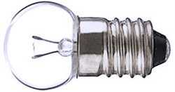
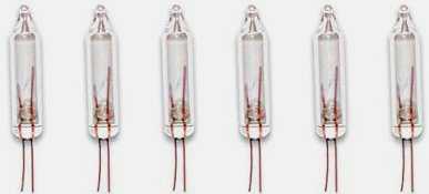
The gain is set by the resistors R3 and Lp, which provide negative feedback to the OpAmp. The starting value for R3 is 100Ω, but this may need to be changed. Lp is a 6-Volt 40mA E10 Miniature Edison Screw (MES) torch bulb. E10 means the outer diameter of the screw is 10mm. When fully illuminated, this lamp has a filament resistance of about 150Ω when fully heated, but when cold the resistance falls to about 15Ω. In other words, if you were to apply a constant voltage to the lamp, then the electrical resistance of the lamp changes, depending on the voltage, but it is NOT linear. Here I will use this effect to regulate the output of the oscillator.
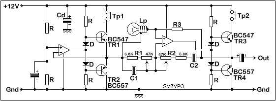
This introduces the next problem: current. The LM358 OpAmp has a maximum output current limit of something like 20mA. This is not sufficient to drive the torch bulb, which requires 40mA, or more. When cold the resistance of the fillament is even lower. So I have added two transistors, TR3 and TR4 to amplify the output current of the OpAmp. Tp2 on the PCB I have added so I can monitor the standing current through TR3 and TR4. In normal operation you must fit a shorting link here. The prototype board needs to have this modification so I can check the design without carving up the PCB.
The oscillator OpAmp requires a split supply voltage. OpAmp1 and TR1/TR2 provide this. Again, TR1 and TR2 must supply enough current to light up the lamp Lp, and Tp1 has been added for the same reason as Tp2.
40 years ago I would not need to play about with TR1, TR2, TR3 and TR4, since there were available low-power thermistors. One model was numbered R53, which was a 10mW 10kΩ thermistor. It didn't take many mA to get it hot. But they were fragile and mounted in a glass envelope, which is why they needed some mechanical protection. Today they are very rare and they cost typically US$35 each.
The R53 thermistor took about 0.5mA at 5 volts, which is only about 2.5mw. A more modern component would need about 0.5 Watt to get it to warm up. A little MES torch bulb is run at about 4 Volts and 15mA, which is about 60mW, or about 10% of the power you would need with a modern thermistor. So there is the reasoning behind the use of the MES lamp - battery drain.
Because of the transistor buffer stages, this circuit should work well with other torch-bulbs, for example 6-V 50mA MES. You can buy a pack of the 40mA MES lamps from Ebay.co.uk for about £5, including postage within Europe. You can even use those 2.7-Volt 50mA Christmas-tree lamps. Sometimes they demand up to 100mA, but it is just to test them, or look at the voltage/power rating. Use whatever you can find, as long as the current is under about 50mA. Up to 100mA and you may have to have more battery capacity, or even reduce the value of the resistors in the bases of TR3 and TR4.
As usual, if I have the luxury of time to plan a project, then there will be a Printed Circuit Board (PCB), if applicable. This is the second PCB that I have layed out using Proteus 7.7. The more I use it, so the more I like it. I wish I had found it 20 years ago.
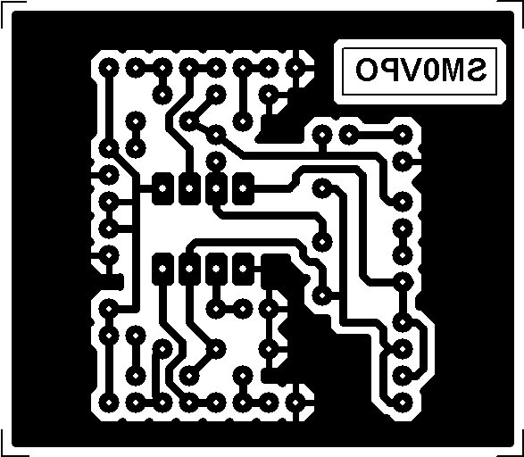
Note that the text "SM0VPO" must be the correct way round when you look at the copper side of the PCB. The above view is looking through the board from the component side, but with x-ray spectacles. Here is the PCB with the component overlay:
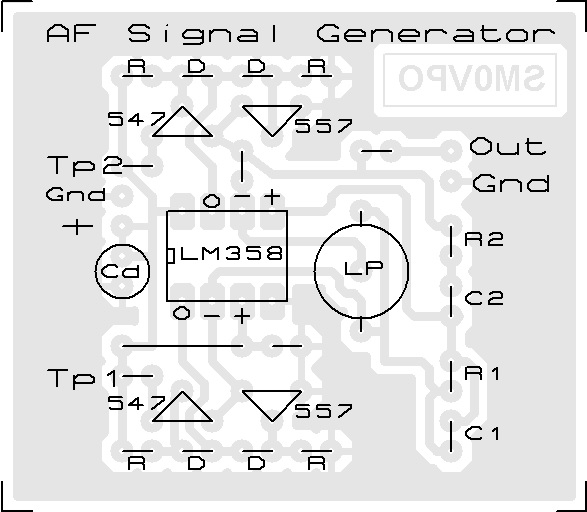
The supply voltage is 12-Volts, DC. The conponents D (x4) are 1N4148 diodes and the cathodes are all at the "SM0VPO" text side of the board. The resistors R (x4) set the standing current through the transistors TR1, TR2, TR3 and TR4. If the values are too low then the voltage drop across the four D diodes may cause the transistors to draw too much standing current. Those at the bottom of the drawing will be about 12KΩ = (1/2 supply volts) x (transistor hfe) / 50mA. Those at the top of the drawing are about 30% of this value (6.8KΩ), because the voltage also contains signal, which varies by +/- 3 volts, or so.
The components marked 547 and 557 are BC547 and BC557. There are two of each.
C1 and C2 connections are connected to a 2-pole, 6-way rotary switch so that different timing capacitors can be selected. You may need to add parallel capacitors in order to get the exact frequency range, but the values I eventually use after the prototype is built will be published here.
R1 and R2 connections are connected to the dual-gang 47KΩ potentiometer, each in series with a 6.8KΩ resistor. These values give the required 5:1 frequency ratio, but as you can see, there is some overlap as the actual resistor ratio is 6.9:1. The desired frequency ranges that I want are:
| Range | Low frequency | Hi frequency | C1/C2 value |
|---|---|---|---|
| 1 | 10Hz | 50Hz | 348.5nf |
| 2 | 50Hz | 250Hz | 69.7nf |
| 3 | 250Hz | 1250Hz | 13.94nf |
| 4 | 1KHz | 5KHz | 3485pf |
| 5 | 5KHz | 25KHz | 697pf |
| 6 | 25KHz | 125KHz | 130pf |
Capacitor values are calculated, so some small adjustment may be needed. Remember that the lowest range, band 1 - 10Hz to 50Hz, will actually cover about 8Hz to 62Hz because of the 7.794:1 resistance ratios of R1 and R2, with reservations for component tolerances. Range 4 (1KHz to 5KHz) should use the same scale as range 1, so C1 and C2 may need to be padded a little to make it so. Also, range 6 capacitor values are so low (139.4pf) that the estimated 8 or 10pf capacitance on the board and wires mean that you will need to drop the value to about 130pf, or so. To be perfectly honest, range 6 is pushing luck a bit.
When I finish the project I may modify the ranges a little. If the slew-rate of the OpAmp causes any distortion at 125kHz, or the actual OpAmp gain falls too much, then I will take a look at the ranges once more. According to the OpAmp data I am "sailing a bit close to the wind", depending on the output amplitude. My target is 1-Volt RMS (2.8-Volts Peak-to-Peak). I really want 10Hz to 50kHz, but if I have to take them all down by 50%, then a lower frequency of 5Hz can still be a useful value. This is the sort of thought I usually have with many of my projects, but after the prototype is built and the working data chosen, I publish actual performance and say nothing ;-).
Ok, testing a prototype can mean some precautions. In this case, remove the links Tp1 and Tp2. Apply 12-Volts to the board in series with a 47 Ohm resistors, and check the supply current is as expected for an OpAmp. It should be about 20mA. Insert Tp1 link and it should rise a little, about 0.5mA. Insert Tp2 link and it should rise by about 1.5mA.
If the current rises by something like 40mA or more, then it means that TR1 and TR2 or TR3 and TR4 are biased too heavily. If this happens, then the diodes marked D may have to be replaced with low-value resistors, of about 270Ω for TR1 & TR2, or 100Ω for TR3 and TR4. The idea is to get TR1 and TR2 to be almost conducting, and the same with TR3 and TR4. Diodes would be nice to have as they have an (almost) constant voltage drop. But if resistors have to be used, then each resistor must drop about 0.65-Volts. It doesn't matter too much if there is any crossover distortion because if the transistors are not conducting then the open-loop gain of the OpAmp(s) will be something like 100,000. The emitters of the transistors will be noise-less due to the negative feedback during transistor conduction.
If all is well, then you can remove the 47Ω resistor from the power supply and connect the 12-Volts directly. You may see the MES lamp light up dimly. This is how it should be with about 1-V RMS of audio at the output. The 100Ω resistor by pin 6 of the LM358 can be adjusted to give you other output voltages, and some adjustment may be necessary if you use a different MES lamp.
The "Out" and "Gnd" connections are the audio output. The component feeding the Out pin is a 220μf capacitor, with the +ve terminal to the emitters of TR3 and TR4. A 4.7KΩ potentiometer should be sufficient for an output level control. I had thought of using another OpAmp to give a low impedance at all output levels, but decided that a low impedance source is not my priority. If that should change, then I will modify the board and include one. Another project for the future ;-).
The prototype was built and it didn't work. I had forgotten two tracks. But on the bright side, this was detected BEFORE I pubished the theoretical project, the the PCB above is, and always was, the correct board layout.Prototype
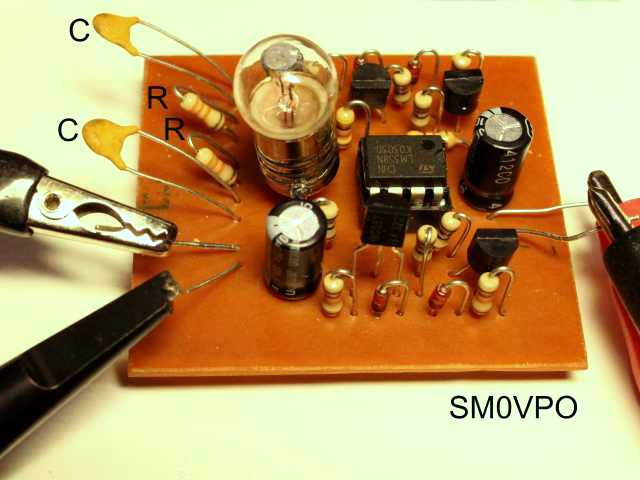
Above you can see the prototype. I used SRPB (bonded paper) board since it is cheap stuff and I have a load of it. Perfect for a board that is likely to be hacked about. In this case, it wasn't, so this board will go in my final project box. The two resistors and capacitors marked C, C, R and R are the timing components (C1, C2 R1 and R2 in the circus diagramus confusicus): I temporarily fitted fixed components to the PCB.
One thing to remember is that C1 and C2 MUST NOT be ceramic capacitors. Ceramics have a HUGE capacitance variation with temperature. At room temperature a 10n capacitor can be anything from 8nf to 12nf. Plonk a soldering iron on it and the capacitance can vary by more than 90%, less than 1nf. In the final box I will mount the capacitors on the range switch and I will also use a 4K7 log output level pot.
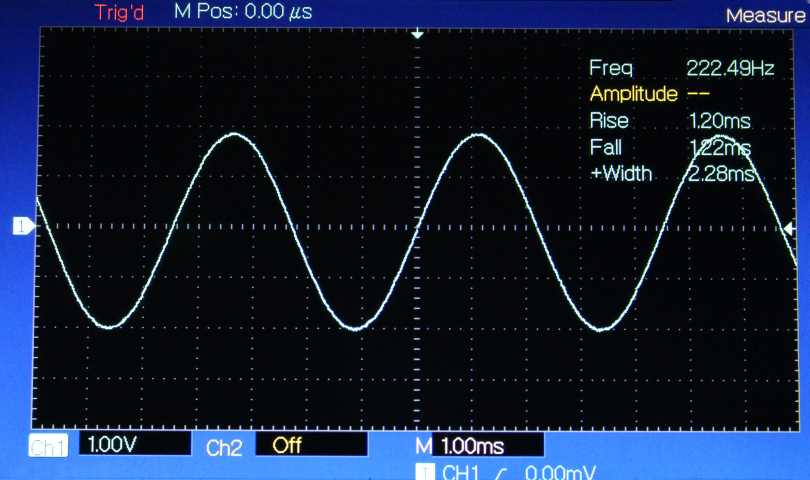
Looking at this oscillator on the oscilloscope you can see the output waveform is constant and a nice clean sine wave. There is a bit of noise, but that is a "feature" of this oscilloscope. When I use the audio spectrum analyser in my mobile telephone it shows that the harmonic distortion is about -53dB, which is about 0.2% THD. That is far better than I had originally hoped for, but with Android apps you can often take accuracy "with a pinch of salt".
I may add a complete photo of the final instrument when it has been stuffed in a project box. If you have any good ideas or suggestions then do not hesitate to contact me.
I hope that this project has given you some "food for thought". You can always e-mail me at harry.lythall@[my domain].com. You can even use oeieio@hotmail.com or hotmail@sm0vpo.com as they are both valid e-mail accounts for me ;-) although I would prefer that you visit my messageboard if you have any questions about this or any other project. I always look forward to receiving feedback, positive or negative ☺
Very best regards from Harry Lythall
SM0VPO (QRA = JO89WO), Märsta, Sweden.