
One of the frequently asked question I recieve is about transistor biasing; "What DC conditions do I need for a transistor to operate?" is one typical question. Well here I will present a little basic information but without any heavy mathematics, all you need to be familiar with is Ohm's Law.
Firstly, consider a typical NPN transistor. It has three terminals: COLLECTOR, BASE and EMITTER. These are often abreviated to C, B and E. Here is the circuit symbol I use for a NPN transistor and a typical transistor (somewhat enlarged).
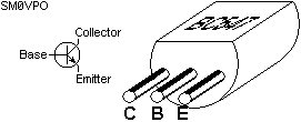
A PNP transistor would have the arrow pointing towards the centre.
(memory jogger - POINTS not points to CENTRE)
Current flows between the Collector and the Emitter, if a current is made to flow between the Base and the Emitter. If there is a Collector current and NO Base then the transistor is said to have a "leakage current".
Ignoring "leakage current", the current flowing between the Collector and Emitter is equal to the current flowing between the Base and the Emitter multiplied by a certain number which is given as "hfe" in the transistor data. Typical value for "hfe" is 200 for a small-signal transistor and 50 for a power transistor.
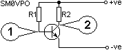
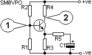
The resistor R1 controls the supply current to the base of the transistor and the transistor collector current flows through R2. The standing voltage at test point TP1 will always be typically +0.7 volts with respect to the emitter although this may vary with different types of transistor:
| Type | Typical | Vbe |
|---|---|---|
| NPN Silicon | BC547 | +0.7v |
| PNP Silicon | BC557 | -0.7v |
| NPN Germanium | OC141 | +0.15v |
| PNP Germanium | OC71 | -0.15v |
| NPN Sil. Darlington | BD679 | +1.4v |
If the supply voltage were 10.7 volts and a BC547 (2N2222) were used above, and we choose 100K ohms for R1, this would give us a base current of 100uA or 0.1mA (I=E/R) using basic Ohms law. The +0.7 volts is subtracted from the +10.7v supply voltage.
The collector current should be hfe x Ib = 200 x 0.1mA = 20mA. If we wanted the transistor to act as an AF amplifier then the 20mA should give us about half the supply voltage (+5.7v) at TP2 so applying Ohms law again we have R=E/I = 5v/20mA =250 ohms. The transistor hfe would be affected by temperature and the base current would also be altered by changes in the supply voltage, so clearly this circuit would be quite unstable in reality. We could stabilise it by changing the biasing a little bit, as shown below:
With +5.7v at the top of R1 and +0.7v at the bottom then the base current would be 50uA (0.05mA). The hfe is still 200 so we will have only 200 x 0.05mA = 10mA for collector current.
By applying Ohms law yet again we have R2=E/I = 5v/10mA = 500 ohms.
Any increase in the Collector voltage would cause the Base current to rise, the Collector current would then rise and due to a higher voltage across R2, the Collector voltage would fall back towards the correct value.
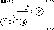
In practice you could make a nice little preamplifier with this circuit. Couple the input signal into TP1 via a capacitor and take the output signal from TP2 via another capacitor. This circuit will work from about 2Hz through to 30MHz. With a suitable component layout it could be extended to over 150MHz.
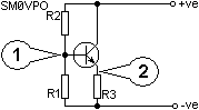
The previous circuit cannot be readily controlled when it comes to voltage gain. The classic textbook "auto-bias" can be quite easily controlled:
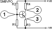
R1 and R2 form a voltage divider from the supply voltage. I will pick R1=10K and R2=40K and use a 10v battery supply.
R1 and R2 will give us +2.0v at the base of the transistor. The Emitter will therefore operate at 2.0v - 0.7v = +1.3v DC.
If we wanted the transistor collector current to be 10mA then the emitter resistor R3 = E/I = 1.3/10mA = 130 ohms.
The transistor collector can therefore vary between +10v and +2v. The mean level is therefore +6v so R4 must develop 10 - 6 = 4 volts. R4 = 4v/10mA = 400 ohms.
In practice you would normally work backwards since the output impedance of the circuit is usually more important. This will determine the value of R4. R1 and R2 in my example total 50K so that they will be drawing 0.2mA from the supply. This should normally be set to at least 10 times the base current:
If hfe = 200 and our Collector current is 10mA then Ib = 10mA/200 = 50uA. R1 and R2 should have been set to draw at least 500uA (0.5mA) from the battery so their values would have to be R1=20K and R2=80K maximum. Lower values will reduce the input impedance of the stage.
In the previous circuit, we finished with R3=130R and R4=400 ohms. Any current through R4 will also flow through R3 so signals will be developed across both resistors. The signal developed across R3 is in oposition to the input so it has the effect of cancelling out a proportion of the output.
The gain of that circuit is approximately equal to R4/R3. In our example this would be set to 400 / 130 or a voltage gain of 3.
As shown above, R3 can be shunted by R5 to reduce its value and increase the gain. C1 prevents the DC bias conditions from being disturbed by R5. If R5 were also 130 ohms, then R5 and R3 in parallel would equal 65 ohms. This would set the gain of the amplifier to 6.
The transistor does not have to be used in the "common Emitter" mode as has been shown so far in this article.
Here the transistor is used as a simple current follower. The DC voltage at TP2 will always be 0.7 volts lower than the voltage at TP1. This may be used for DC or AC applications by suitable coupling. If used for AC coupling then R1 and R2 would be about equal value with R2 being slightly lower of the two values.
It may be that the output circuitry of a simple amplifier is to have an inductive load. In this case the collector load resistor is replaced by an inductor or transformer primary winding.
If however the circuit was not used to amplify a linear circuit where distortion is acceptable, or even required (frequency multipliers for example) then R1 and R2 only need to be changed in value.
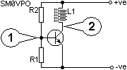
An emitter resistor would only need to be inserted in order to limit the transistor current. R1 and R2 would be set to provide about +0.7v at the base of the transistor for Class AB or class B operation. For Class C operation then R2 could be permanently removed.
If an NPN and PNP are used together in the Common Collector mode (see Current gain above) then a linear current amplifier has been created. Often known as a "complmentary" output stage. If preceeded with a voltage amplifier then a power amplifier has been created.
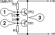
TP3 should be set to half the supply voltage for linear operation by selecting R1 and R2 of equal values. This gives us a small problem: If the supply is, say, 10v and TP3 is set to 5 volts, then considerable distortion will occur. This is because TR2 base will require +5.7v or more to make it conduct and TR1 will require +4.3v or less to make it conduct. This means that the input signal can vary by 1.4 volts without the output changing.
One solution is to include a pair of diodes of the same material as the transistors (silicon, germanium) to create a DC offset. With simple silicon transistors the DC voltage between TP1 and TP2 will be the sum of both TR1 and TR2 base-Emitter turn-on voltages. The voltage level is very critical. A few millivolts too much and current will flow directly through TR2 and TR1 liberating much heat and possibly destroying the two transistors. This can be controlled to some extent by adding emitter resistors to TR1 and TR2:
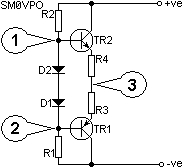
R3 and R4 will help to limit the current drawn by the transistors especially when they are hot and the Base- Emitter turn on voltage has reduced. It is for this reason that many such circuits use a temperature compensation network in the basebiasing circuitry.
Ok then, that should answer just about all the questions I have received so far and without any mathematics, other than Ohms Law. If you want further information then go to your local technical library or bookstore.
Return to INFO page