
A Programable Logic Array (PLA) is in reality a very small memory chip, often of the fusable link variety. We can have exactly the same functions in an EPROM and have more space left over for even more complex functions.
The simplest application of an EPROM is to read a predetermined code as an instruction for a microprocessor. We can use this ability to store data to make a PLA to give a particular logic function. Imagine for a moment that you simply want to make a binary NAND gate: Draw the truth table and list the input terminal in binary-numerical order. These are the address terminals of the EPROM and the output is a data terminal:
| Address | Data | 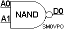 | ||
|---|---|---|---|---|
| Hex | Bits 7 6 5 4 3 2 1 0 |
Bits 7 6 5 4 3 2 1 0 | Hex | |
| 00h | 0 0 0 0 0 0 0 0 | 0 0 0 0 0 0 0 1 | 01h | |
| 01h | 0 0 0 0 0 0 0 1 | 0 0 0 0 0 0 0 1 | 01h | |
| 02h | 0 0 0 0 0 0 1 0 | 0 0 0 0 0 0 0 0 | 01h | |
| 03h | 0 0 0 0 0 0 1 1 | 0 0 0 0 0 0 0 0 | 00h | |
In this example A0 and A1 are the inputs to the NAND gate and D0 is the output terminal. Note that the right-hand binary digit is the least significant digit and the numerical values will be given in Hexadecimal. As you can see, there are four combinations. Now let us add another NAND gate to the same EPROM:
| Address | Data | 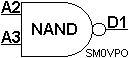 | ||
|---|---|---|---|---|
| Hex | Bits 7 6 5 4 3 2 1 0 |
Bits 7 6 5 4 3 2 1 0 | Hex | |
| 00h | 0 0 0 0 0 0 0 0 | 0 0 0 0 0 0 1 0 | 02h | |
| 04h | 0 0 0 0 0 1 0 0 | 0 0 0 0 0 0 1 0 | 02h | |
| 08h | 0 0 0 0 1 0 0 0 | 0 0 0 0 0 0 1 0 | 02h | |
| 0Ch | 0 0 0 0 1 1 0 0 | 0 0 0 0 0 0 0 0 | 00h | |
For BOTH the NAND gates to work at the same time we must therefore consider all possible binary address combinations of both tables. This means copying the first table into all four possible combinations of the second table:
| Address | Data | 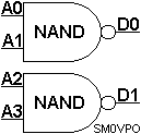 | ||
|---|---|---|---|---|
| Hex | Bits 7 6 5 4 3 2 1 0 |
Bits 7 6 5 4 3 2 1 0 | Hex | |
| 00h | 0 0 0 0 0 0 0 0 | 0 0 0 0 0 0 1 1 | 03h | |
| 01h | 0 0 0 0 0 0 0 1 | 0 0 0 0 0 0 1 1 | 03h | |
| 02h | 0 0 0 0 0 0 1 0 | 0 0 0 0 0 0 1 0 | 02h | |
| 03h | 0 0 0 0 0 0 1 1 | 0 0 0 0 0 0 1 0 | 02h | |
| 04h | 0 0 0 0 0 1 0 0 | 0 0 0 0 0 0 1 1 | 03h | |
| 05h | 0 0 0 0 0 1 0 1 | 0 0 0 0 0 0 1 1 | 03h | |
| 06h | 0 0 0 0 0 1 1 0 | 0 0 0 0 0 0 1 0 | 02h | |
| 07h | 0 0 0 0 0 1 1 1 | 0 0 0 0 0 0 1 0 | 02h | |
| 08h | 0 0 0 0 1 0 0 0 | 0 0 0 0 0 0 1 1 | 03h | |
| 09h | 0 0 0 0 1 0 0 1 | 0 0 0 0 0 0 1 1 | 03h | |
| 0Ah | 0 0 0 0 1 0 1 0 | 0 0 0 0 0 0 1 0 | 02h | |
| 0Bh | 0 0 0 0 1 0 1 1 | 0 0 0 0 0 0 1 0 | 02h | |
| 0Ch | 0 0 0 0 1 1 0 0 | 0 0 0 0 0 0 0 1 | 01h | |
| 0Dh | 0 0 0 0 1 1 0 1 | 0 0 0 0 0 0 0 1 | 01h | |
| 0Eh | 0 0 0 0 1 1 1 0 | 0 0 0 0 0 0 0 0 | 00h | |
| 0Fh | 0 0 0 0 1 1 1 1 | 0 0 0 0 0 0 0 0 | 00h | |
It is all very easy using squared paper and a highlighter pen to mark the vertical columns.The final code for the Dual NAND gate PLA is therefore given below with the EPROM start addresses at the left hand side in bold.
| 0000 : | 03 03 02 02 03 03 02 02 |
|---|---|
| 0008 : | 03 03 02 02 01 01 00 00 |
One other VERY important point, with even a small EPROM we have used only two data terminals and four address terminals, this leaves at least ten address pins and six data pins left for yet more logic functions. What's more, these logic functions can be made inter-related so that the function of one gate can change, depending upon the input conditions to another! Now, is that a powerfull tool or is it just a powerfull tool?
Many logic functions require a latching function, that is the gate will remember a logic state. Easy - peasy! The task; I want to make a simple SET/RESET latch. This has two inputs. If the first input is briefly given a short positive pulse, will set the output high (1) and stay there, even when the pulse has gone. I also want another input which, if it receives a short positive pulse, will reset the output back to "0" again. I also want a second output that is the opposite polarity to the first output.
For my two inputs I will use A0 and A1. My output will be from D0, and it's complement will be A1. To make the EPROM remember a condition we must allow the device to control itself to set up a stable state. Connect the D0 output to the A2 input on the circuit board, now let us consider the program. There are three inputs, A0, A1 and A2, therefore there are only a total of 8 memory locations that need to be programmed.
| Address | Data | 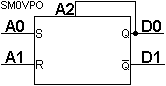 | ||
|---|---|---|---|---|
| Hex | Bits 7 6 5 4 3 2 1 0 |
Bits 7 6 5 4 3 2 1 0 | Hex | |
| 00h | 0 0 0 0 0 0 0 0 | 0 0 0 0 0 0 1 0 | 02h | |
| 01h | 0 0 0 0 0 0 0 1 | 0 0 0 0 0 0 0 1 | 01h | |
| 02h | 0 0 0 0 0 0 1 0 | 0 0 0 0 0 0 1 0 | 02h | |
| 03h | 0 0 0 0 0 0 1 1 | 0 0 0 0 0 0 1 0 | 02h | |
| 04h | 0 0 0 0 0 1 0 0 | 0 0 0 0 0 0 0 1 | 01h | |
| 05h | 0 0 0 0 0 1 0 1 | 0 0 0 0 0 0 0 1 | 01h | |
| 06h | 0 0 0 0 0 1 1 0 | 0 0 0 0 0 0 1 0 | 02h | |
| 07h | 0 0 0 0 0 1 1 1 | 0 0 0 0 0 0 0 1 | 01h | |
Just look at the input binary pattern and consider what you want it to do for each possible combination. With both A0 and A1 low (0) then the output should be "2" so that D1 is the "NOT0". If A1 becomes a "1" then that location of memory contains "01" which sets D0 output to +5volts. Since D0 is also wired to A2 in the circuit then the EPROM will change it's own address by adding A2. This will cause the EPROM address to jump from "01" to "05". When the input pulse goes the address will change to "04" and that location also keeps D0 high. If you input a high to A1 then the address will become "06" and that location contains the data "02". The output is therefore low again and so the EPROM will change it's own address from "06" to "02".
The addresses "03" and "07" gave a small problem since this binary combination means both set AND reset! So what do we do? As you can see, I did nothing. If D0 was already a "1" I left it there, but if it was "0" I also left it there.
If it all sounds complicated, read that through a few times and it should become clear enough. If you did understand it all then try to make up a PLA for two NAND gates and a SET/RESET latch! This will need only 7 address pins and 3 data output pins so the EPROM is still far short of it's capacity. The code will only occupy address locations 0000h to 007Fh or 128 bytes, so even the smallest of EPROMS will hold quite a lot of code. Now you have the ability to create your own complex logic functions using cheap EPROMs.
I hope that you understood all of that. Now I will get back to the workbench and do some work on the next project and destroy a few more EPROMS.
Have fun and best regards from Harry
Return to INFO page