

Well, here it is at last, the SM0VPO EPROM burner. With my EPROM burner you will be able to burn your own EPROMS and continue with some of the projects described, and those yet to come on my homepages. I have tried NOT to use any weird or expensive chips in this project, so this programer can be built in countries where there is restricted access to logic chips. Transistors used are generic NPN and PNP types, such as the 2N2222 or BC547 (NPN) etc. I have NOT made use of the selectable EPP and ECP functions available on modern computers, so this card will be compatible with your old 286 computer. There will be no speed advantage in using a modern 750MHz computer since the software has to slow it down to burn each address for 50mS (+/- 5mS), but the software will accomodate a faster computer. This means that it will work almost as fast using your old 8MHz 286 machine gathering dust in the loft.

The EPROM progrogramer does NOT use any device to output a voltage to the PC printer port, only a current sink. All inputs from the printer port are buffered. In this way there is little or no possibility of damage to the printer port, even with most wiring error possibilties during construction. This EPROM burner will handle most standard EPROMS, but some switching may be required by the constructor at the EPROM socket. I will leave that up to you, although I do give some advice on this subject. Please note, the software I have written is NOT suited for the more recent EPROMS that only require 10mS or the shorter "blow until burnt" programing pulses. The basic circuit shown in this article will allow the programing of the following generic EPROMS:
| Type | Size | VPP volts | ||
|---|---|---|---|---|
| 2716 | 2K x 8 | 12.5v | 21v | 25v |
| 2732 | 4K x 8 | 12.5v | 21v | 25v |
| 2764 | 8K x 8 | 12.5v | 21v | 25v |
| 27128 | 16K x 8 | 12.5v | 21v | 25v |
| 27256 | 32K x 8 | 12.5v | 21v | 25v |
| 27512 | 64K x 8 | 12.5v | 21v | 25v |
| 271001 | 128K x 8 | 12.5v | 21v | 25v |
If you were to fit a 40-pin socket then there is no reason why you cannot program the 271001, 271024, 272001 and the 274001 EPROMs. Please note that some of the above packages and programing voltage may not be available, but the possibility to program them exists with this burner. I will give you some common chip manufacturer and programing voltages further down in the article. Here is a photograph of the prototype main board. As you can see I have used a prototyping "blob board".
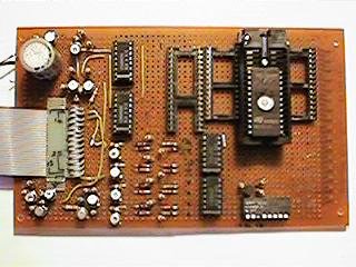
As you can see I have used a prototyping "blob board", so there is no PCB foil pattern for this project. Since I am not going to be making a kit, nor will I ever build more than one of them (I saw no point in all that hard work - I'm a lazy gitt!). Now I can get on with other projects. The board wiring technique I used is like this. It will allow you to build the board in stages and test each stage. An oscilloscope is nice to have, but you can test it with just a voltmeter and slow down any timing loops.
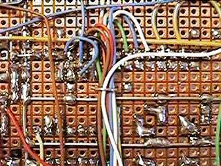

The main logic card addresses the EPROM and processes signals to and from the computer. I have soldered a 25-way ribbon cable to the 25-way printer port plug. The other end is terminated directly to the main board with a bit of off-cut PCB for strain relief. As you can see in the photograph, there is not much logic the board so construction could be quite fast. The programing software writes data to ports 0378h, 0379h and 037Ah. These are the hexadecimal addresses of LPT1, the parallel printer port. The software uses the following connections to the computer. Pin# indicates the pin numer of the 25-way D-sub printer port connector used on the PC computer. The Sense indicates whether the input/output of the computer printer port is normal (+ve) or inverted (-ve). Intended function gives a clue as to how the port is normally used by computers.
| Pin# | EPROM burner use | Sense | Intended function |
|---|---|---|---|
| 2 | Read data MUX select | +ve | 0378 bit 1 - Data word to printer |
| 2 | Data word D0 to EPROM | ||
| 3 | Data word D1 to EPROM | +ve | 0378 bit 1 - Data word to printer |
| 4 | Data word D2 to EPROM | +ve | 0378 bit 2 - Data word to printer |
| 5 | Data word D3 to EPROM | +ve | 0378 bit 3 - Data word to printer |
| 6 | Data word D4 to EPROM | +ve | 0378 bit 4 - Data word to printer |
| 7 | Data word D5 to EPROM | +ve | 0378 bit 5 - Data word to printer |
| 8 | Data word D6 to EPROM | +ve | 0378 bit 6 - Data word to printer |
| 9 | Data word D7 to EPROM | +ve | 0378 bit 7 - Data word to printer |
| 15 | Mux D0/D4 from EPROM | +ve | 0379 bit 3 - Printer control (status) |
| 13 | Mux D1/D5 from EPROM | +ve | 0379 bit 4 - Printer control (status) |
| 12 | Mux D2/D6 from EPROM | +ve | 0379 bit 5 - Printer control (status) |
| 10 | Mux D3/D7 from EPROM | +ve | 0379 bit 6 - Printer control (status) |
| 1 | Address counter advance | -ve | 037A bit 0 - Printer control (readback) |
| 14 | Address counter reset | -ve | 037A bit 1 - Printer control (readback) |
| 16 | EPROM chip-enable (CE) | +ve | 037A bit 2 - Printer control (readback) |
| 17 | Program VPP on/off | -ve | 037A bit 3 - Printer control (readback) |
You will note that there are eight pins from the computer to the EPROM burner card, but there are only four pins available as input to the computer. All four signalling pins at 037Ah have been used, so the PC data out D0 (pin 2) has also been used as a high/low mulitiplex (Mux) nibble selector. The four signalling pins do not begin with bit-0, they begin with bit-4. The software makes corrections for this byte address difference. Bit-7 is not used in this circuit, but this is also masked (EXORed) in the software.

Now we come to the interesting 'nitty gritty' EPROM burner card circuit diagram. As you will see in the circuit below, safety of the computer was my main concern. I have therefore used transistors to buffer signals between the card and the PC. NO voltage is fed from the burner card to the computer. The price is a few transistors, but they are cheap enough. All the connections to the left of the circuit and prefixed with a "B" are the D-25 printer port terminal pins on your computer. All the connections to the right of the circuit are to the EPROM.
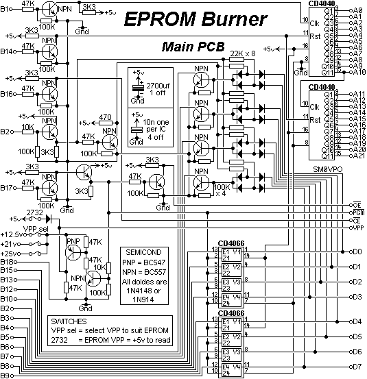
The 'STROBE' output from the computer (D25 pin 1) is connected to the clock input of the first CD4040 counter chip. Clocking this pin causes the binary counter to advance. The output of the counter is therefore a binary number capable of addressing EPROMS up to 2732 (0 to 4095). The last output of this counter is the carry to the second CD4040 counter so that we can extend the count far beyond any commercially available EPROM, at the time of writing this article. The RESET output from the computer (D25 pin 14) is connected to both the CD4040 counters so that they can be reset to zero.
Now that we have addressed the EPROM we need to ENABLE the EPROM and read the data from it. As I mentioned earlier, there are only four input pins to the computer (D25 pins 15, 13, 12 and 10). First we read the EPROM D0, D1, D2 and D3, then we read the other nibble; D4, D5, D6 and D7 by changing the diode switches into the buffer transistors. The diode data selector is controlled from the computer output data D0 (D25 pin 2). There is no output data from the computer during an EPROM read operation, so the eight data pins are free for signalling.

As regards VPP switching, I have fitted a DIP switch to the main card, from which I selected the VPP programming voltage. This could be a dangerous thing to do since it is possible to connect, for example, the +25v supply directly into the +12.5v supply. I reasoned that I know what I am doing and so I will have more sense that to do something so stupid. If you wish to build this circuit for someone else to use, then perhaps you should fit a rotary switch. There is just one anomoly I noticed with EPROMS, that VPP should be 0v for everything except writing data for all EXCEPT the 2732. This requires +5v on pin 20 which is then raised to the programming voltage during the burn. A DIP switch has been used to select this.
You do not need to select any other switches to burn a particular EPROM type, just plug it into a different socket. You could economise on sockets by using the same 24-pin for both 2716 and 2732 by adding switching:
| Pin | 2716 | 2732 |
|---|---|---|
| 20 | /OE | VPP |
| 21 | VPP | A11 |
The 28-pin socket will already program 2764 and 27128 without modification since pin 26 (A13) is not used on the 2764. You will therefore need to fit one or more of the following sockets. It may be that you do not need to program every type of EPROM, therefore you can skip some of them, as I did. If you are also clever at switching then you could use a single 32-pin socket and fit each EPROM to the BOTTOM (see the photograph).
| Socket | EPROM types |
|---|---|
| 24-pin | 2716 2732 (see text above) |
| 28-pin | 2764 27128 (no switching) |
| 28-pin | 27256 |
| 28-pin | 27512 |
| 32-pin | 271001 27001 |
Use ordinary IC sockets but you can plug a Zero Insertion Force (ZIF) socket into one of the IC sockets to suit the EPROM you want to burn. Now you need to know the pin-outs of the major types of EPROM. Here they are in all their glory.

The PSU uses a single transformer ripped out of a bedside radio and having a 10-0-10v secondary. It provides the following voltages:
| Voltage | Current | Used for: |
|---|---|---|
| +25v | 20mA max | VPP during programming |
| +21v | 20mA max | VPP during programming |
| +12.5v | 20mA max | VPP during programming |
| +5/6v | 200mA max | VCC for the EPROM chip |
| +5v | 50mA max | VCC for the logic circuits |
The card below is the PSU card which provides 5v, 5/6v, 12.5v, 21v and 25v DC. The 5/6v output is software controlled since most EPROMS having a 12.5v VPP programing voltage require the +5v line to be increased to +6v during the programing pulse.
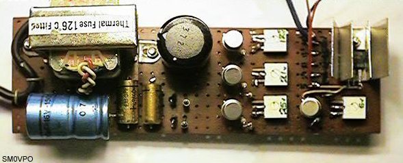
The 5/6v switching is done by the software, but it has to be selected on the main PCB. The only chips used here are LM317T voltage regulator chips, but these can be replaced using Zener diodes and series regulator transistors, if you have difficulty getting these chips. Here is the circuit diagram of the PSU card.
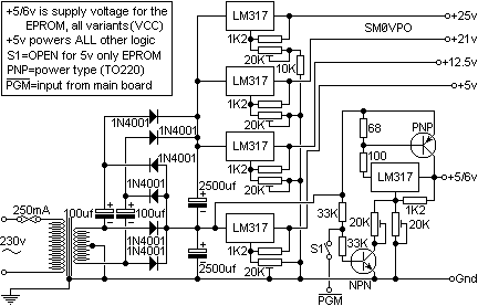
As you can see, there is nothing particularly clever about it. There is a simple full-wave rectifier, but there is also a double Cockroft ladder to give 3x the output voltage. With a 9v-0-9v secondary transformer it was just possible to get the full 25v VPP but I recomend you use a 10v-0-10v transformer. The rectifiers are followed by a whole bunch of regulators. It would perhaps have been simpler to have used a load of switching but if you switch the pot in a standard LM317 regulator and a wire breaks then the volts goes to maximum. Again I prefered safety to simplicity. The only thing to be wary of is the 5/6v switching derrived from the /PGM terminal on the main burner board. This requires some alignment.
Now you have a good basis for experimenting so I hope that you have fun. If you decide to build it then I suggest you build it in stages, beginning with the PSU, EPROM addressing and EPROM reading. Always test before you plug an EPROM in.

I built mine in stages. I began with the PSU, then took a blank bit of "blob board for the main board. Connect the 25-way ribbon cable to the D-range plug and terminate the other end on the board. Mark the strain-relief plate for the cable with the fin numbers to help you. Don't forget that each wire in the cable is alternately numbered; 1, 14, 2, 15, 3, 16, 4, 17, etc. This probably took me as long to build as the rest of the project! Insert the 2500uf cap and hook up the +5v line to the cap and connect the ribbon cable earth (B18) to the -ve. Now we are ready to begin the logic.
The transistor buffers at B1 and B14 are fitted first, then fit the two CD4040 chips and test them out. You can use the following code in GW-BASIC to output commands to test the hardware. A small tip, copy/paste this code from your browser to NOTEPAD and save as TEST.BAS which can be opened by GW-BASIC or Turbo Basic (TB).
| 100 REM: Test CD4040 clocking |
| 110 OUT &H037A,&H0 |
| 120 GOSUB 1000 |
| 130 OUT &H037A,&H1 |
| 140 GOSUB 1000 |
| 150 IF INKEY$="Q" or INKEY$="q" THEN END |
| 160 GOTO 110 |
| 170 OUT &H037A,&H2 |
| 180 GOSUB 1000 |
| 190 OUT &H037A,&H0: END |
| 1000 REM: Delay loop - adjust to suit test and computer speed |
| 1010 FOR X=0 TO 2000 |
| 1020 NEXT X |
| 1030 RETURN |
When you type RUN 100 the program will begin toggling the D25 pin 1 up and down (0 - 5v). You can then look at the output pins of the two CD4040 chips. Each pin should be filcking up and down half as fast as the previous pin. Change the number 2000 in line 1010 to 64000 if you want it to flich really slowly or change it to 10 if you want it to flick faster to check the higher-order outputs of the CD4040 chips. Simply pressing "Q" will stop the program and the CD4040 counters will stop counting. Type CONT and they will continue. Type RUN 170 and check the counter chip pins all reset back to 0-volts.
Now insert the four NPN transistors and buffers that are connected to B2, B2, B10, B12, B13 and B15. Yes, there are two contacts named B2, these go to the same wire of the ribbon cable. When you have wired them up, switch on the PSU and enter the following code to the code you have already written.
| 200 OUT &H37A,&H2 |
| 210 OUT &H37A,&H0: A1=15-INT(INP(&H379)/8) |
| 220 OUT &H37A,&H4: A2=15-INT(INP(&H379)/8) |
| 230 LOCATE 1,60: PRINT A1: LOCATE 1,70: PRINT A2 |
| 240 GOSUB 260: GOTO 210 |
| 250 END |
| 260 FOR X=1 TO 100: NEXT X |
| 270 A$=INKEY$: IF A$="" THEN RETURN |
| 280 IF A$="N" THEN OUT &H37A,&H1: OUT &H37A,&H0: RETURN |
Type in the command RUN 200 and you will see two numbers to the top right of the screen. These two numbers should be "F" and "F" if the circuit is working. If the circuit has no power then you will see "0" and "0". Assuming all is well, you can individually short to ground the data terminals (D0 through D7) that will be connected to the EPROM. When you do this the numbers will change, depending upon which pin you have grounded. You can use this to identify the data terminals, it can save you a bit of time when building. To stop the BASIC program running simply press any key. If you are using a 700MHz computer (you lucky, lucky bastard) then you may have to change the number in the program line 270 from 100 to 2000 or more to give the hardware time to keep up with your computer. You can use an oscilloscope to monitor the voltages on the two 22K resistors (directly under the words Main Board in the circuit diagram) and see them toggling alternately. If you only have a voltmeter then change the number in the program line 270 from 100 to 20000 and they will be slowed down so you can see them switching.
Next, wire in the transistor buffer connected to B16 and leading to the /CE of the EPROM. To test this you do not need any additions to the program, just put a voltmeter between the /CE terminal and the ground. Type the BASIC command "OUT(&H037A),0" in immediate mode and the voltmeter should show +5 volts. Type the BASIC command "OUT(&H037A),4" in immediate mode and the voltmeter should show 0 volts. If this is working then you could wire the EPROM socket and read data from the EPROM.
Finally, connect all the circuitry associated with B17, +5v, +12.5v, +21v, +25v, /OE, /PGM and VPP. Switch only ONE of the voltage selectors ON (+25v) and run the following program from GW-BASIC. Again, copy the text into TEST.BAS opened with NOTEPAD.EXE and copy it into the previous program examples you have already written.
| 300 OUT &H37A,&H0 |
| 310 GOSUB 1000 |
| 320 OUT &H37A,&H8 |
| 330 GOSUB 1000 |
| 340 IF INKEY$="Q" or INKEY$="q" THEN END |
| 350 GOTO 300 |
You should see a +5v square-wave on the /OE and /PGM terminals. You should also see a +25v square-wave signal on the VPP signal. Again, if you do not have an oscilloscopy, change line 1010 to read 1010 FOR X=0 TO 20000 and you will see a slow ON/OFF switching that can be read on a voltmeter.
Now we come to the final logic stage, presenting the WRITE data to the EPROM. Wire in the two CD4066 chips and the circuitry between them and B2, B3, B4, B5, B6, B7, B8 B9, D0, D1, D2, D3, D4, D5, D6 and D7. To test them out, run the following program and check that there is a pulse on D0, then D2, then D3 etc. The pulse is in sequence and should be off/on with a ratio of 7:1.
| 360 OUT &H37A,&H8 |
| 370 Z=1: FOR Y=1 TO 8 |
| 380 OUT &H378,Z: Z=Z*2 |
| 390 GOSUB 1000 |
| 400 IF INKEY$="Q" or INKEY$="q" THEN END |
| NEXT Y: GOTO 370 |
Naturally, the program lines must be added to the existing TEST.BAS program we have already built up. Execute this test by entering RUN 360 and exit it by pressing "Q". If you have a multimeter then you should see about 0.7vDC on each D0 to D7 data terminals. You could also increase the value of 200 in line 1010 to 20000 or more to slow it down so you can see it switching. If you have got this far, and it is working, then what are you waiting for? Plug in your blank EPROM and read it using my software. If that works then try writing to it. If that works Ok then wire up the other sockets for the other EPROMS you are interested in.

If you need to know some common EPROM programing voltages then take a look here.

Restart your PC after using the burner software if you want to use your printer. The software may leave the printer port configured in some invalid state that Windoze or Epsom do not like.

I hope that you have some fun programing. Very best regards from Harry - SM0VPO
Return to INFO page