
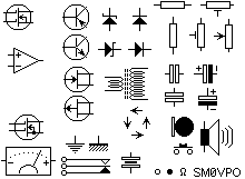
All symbols are saved in this file so I can easily cut'n paste from the file to the new picture. Using the OPTIONS menu, select black & white so the BMP file is relatively small. During the editing it is important that pasted images do NOT wipeout your drawing but the must be transparent. This is shown by the orange arrow below:
Note the tool I have selected. Using this I can position the mouse, click and drag a square. Copy it (Ctrl+C) and then paste the symbol into the circuit you are drawing (Ctrl+V). A typical BMP image will be about 150K, but to convert it to black/white (2 colours) will reduce the size to typically 20K. Use PSP, GWS or any other graphics editor program to open and SAVE-AS = GIF file. The file size will then reduce to about 4K.
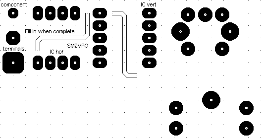
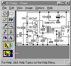
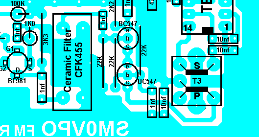
Naturally, I enlarge the page then copy/paste the reference grid to the rest of the page paying attention to alignment of the grid dots. Here there is a choice of pad sizes and I have also included pad form that I created on my last project. They fit the 10mm IF transformers (upper right) and CFK455 ceramic filters (lower right). Copy and save this picture as a BMP file. Open using PC-PAINT then increase the canvas size. Cut'n paste the dots so that they accurately lay on each other and you will have an alignment grid for positioning pads. Let us look at a small part of my latest project, the FM receiver. This is a small corner of it. Notice that I draw it as if I am looking from above the component side.
Pads are placed and joined together with tracks, cut'n paste from the top left corner of the image. Save this image for later (a) in case you want to amend it. I then "spot-out" the alignment point from the center of every hole and fill in. It takes only a couple of minutes:

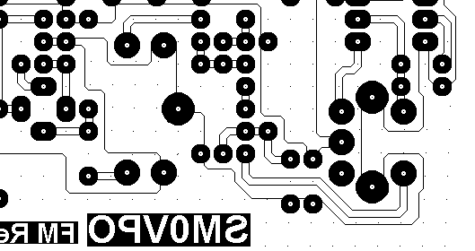
Now save the PCB image (b) then save again with the image attributes as colour (c). You can then fill-in green or any light colour into all the black areas and add the component layout. It looks like this when you have finished:
You will now have three files, one base file, one PCB foil and one component overlay file. To make the artwork for the PCB just print the PCB file (b) to a laser printer with scale set to 39% (on my printer) and check that the holes are 0.1" (2.54mm) appart. You can get plastic film designed for ink-jet printers but for prototype work I use ordinary paper and increase the exposure time. Note that the image must be a mirror of what you want (an x-ray view through the board) so that the correct image appears when the ink is in direct contact with the board. Otherwise light would creep under the film and reduce your line thickness.
As a general rule, always save black/white drawings in GIF format and colour pictures as JPG format. This will give you the smallest files possible.
Well I hope that the above answers your question and saves me having to repeat it all over and over again via E-mail. Have fun with your circuits. Very best regards from Harry - SM0VPO
Return to INFO page