
Ok, so I have done a lot of playing around with the domestic FM band. This will probably be one of the last transmitters for the 88MHz to 108MHz band. This particular TX is of special interest to those wishing to build low power Power Amplifiers for the VHF bands since it used impedance matching, power amplifier and antenna filtering, all of which should be used by radio constructors, whether it be for amateur radio or any other form of radio. The features of this project are:
NOTE - This project is illegal to use or build in many countries. I accept no responsibility what-so-ever for any ilegal use. This circuit is provided solely as an educational project. Now I have got that off my chest, let me get on with the project.
The circuit itself is fairly conventional, with a couple of small refinements. It all begins with TR1 (BC547) in an inverted Hartley oscillator configuration. The feedback to the Base of TR1 is via a small 4.7pf capacitor to help keep the oscillations as weak as possible whilst allowing the oscillator to be a reliable starter. The frequency of the oscillator is determined by L1 and the 22pf trimmer capacitor and functions in the range of about 76MHz to 119MHz using the PCB I have made.
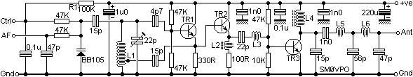
| TR1 = BC547 | TR2 = BC547 | TR3 = 2N3866 or 2N4427 |
|---|
The 15pf capacitor couples the top of L1 to the varicap diode which serves to add more capacitance to the tuned circuit to alter the frequency. R1 adds the supply voltage to the varicap, with a little noise decoupling (the 0.1uf capacitor). If you are to use synthesiser control then it is important to remove R1 from the circuit, then connect the synthesiser loop filter output to the terminal marked "Ctrl". Audio is coupled to the BB105 via a 47K resistor. There is only 47pf of decoupling in order not to restrict the AF bandwidth of the complete transmitter. The AF bandwidth is flat from 3Hz to about 72KHz, but if we look beyond these limits, there is an increase of +6dB at DC. This is because the two 47K resistors divide the AF input voltage by 2, but at DC the 0.1uf capacitor has time to charge, the two 47K resistors do not therefore divide.
TR2 (BC547) is both biassed and directly connected to the Emitter of TR1, which is a little unconventional in a VHF circuit. I needed to get a good input to TR2 and cut down on components. There are already far too many coils as it is in this circuit. Remember that the BC547 is an audio transistor but works well at VHF. The inductor in the Emitter of TR2 helps to extend the response a little to give a bit more signal to drive the final power amplifier transistor (TR3). TR2 gives no voltage gain; it is current we need to drive TR3. We already have enough volts from the oscillator.
22pf and L3 couple TR2 output into the Base of TR3. These components match the impedances so we get the maximum power possible into TR3 Base. The signal level, however is still quite low, so some DC biasing has been added to turn TR3 ON a bit. The transistor should draw about 5mA with no signal. This is not enough to make it become linear, but it is operating around class "B". This would make a very poor frequency multiplier, so harmonics are also reduced a little by the DC bias. Note that NO emitter resistor has been used. The prototype units all worked well without one and the drive level is not enough to cause the transistor to conduct very much. The small standing DC bias of 5mA doesn´t even "tickle" TR3. In operation the DC voltage on the Base of TR1 will be negative due to the drive level, conduction of TR3 Base/Emitter junction and the 22pf capacitor. TR3 does NOT need a heatsink.
If you want to use a different transistor in place of TR3 then I suggest you remove L3 and substitute a current meter in place of L4. Apply volts to the transmitter. The current should be about 5mA. Select the value of the 47K resistor if required. Any current reading between about 2mA to 8mA "will do nicely sir" (even without your American Express card!)
The collector of TR3 (2N4427) has a big (by QRP standards) choke to pass the supply DC, but presents a high impedance to RF. The RF signal is then matched to 50-Ohms with the 15p, L5 and 56p. The 1nf cap simply blocks the supply voltage that would otherwise pass to the antenna. L5 and 56pf form a low-pass filter that helps to block harmonics present in the output signal. L6 and 47pf are added to further reduce the harmonic levels. This filter is an absolute MUST for all transmitters if one does not wish to offend every other user of the radio spectrum. L5 and L6 have also been positioned on the PCB so that there is a little coupling between them. This coupling serves to cancel out any residual signals, not within the passband of the filter, that may be present at the input to L5. It is this effect that was responsible for the unexpected cleanliness of the first prototype, and a little layout experimenting has now reduced the 2nd and 3rd harmonics to -60dBc at all supply voltages. With 150mW output, this corresponds to 3rd harmonic of 150 nano-watts and a 2nd harmonic level of just 50 nano-watts.
I have "played around" with the values and taken a few liberties. If you want to try adjusting the coils then then will be able to get another 2 to 3dB out of the TX. I have deliberately mis-tuned a couple of times in order that impedances and resonances will improve at the edges of the band. The result is that the performance of the transmitter does NOT vary (much) no-matter which end of the band you are operating at.
As you will apreciate, L1 and the tuning capacitors all affect the frequency of the complete transmitter. Winding L1 has therefore NOT been considered. This would result in a spring-like affair that would cause instability, or more precisely, "microphony". This is an effect where the coil wobbles about with very small mechanical movements. In severe cases you can even talk to the the circuit, as any owner of a Marconi TF995 signal generator will testify. By using a coil etched on the PCB you will find that microphony has been eliminated. So has coil expansion with temperature. It must be remembered, however, that this circuit is STILL based upon an LC circuit and therefore subject to changes of frequency with changes of supply voltage and "hand capacitance", etc. I will cover the supply voltage changes shortly.
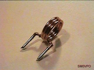
L2 is wound on small ferrite beads. L2 is placed in series with the emitter of the buffer transistor, TR2. In the interests of stability it is very important that this coil does NOT radiate like a loop antenna. It is composed of 4 turns of 0.15mm Dia. enamelled wire (magnet wire in the US). The grade of ferrite is unimportant, as long as it is a grey one. One complete turn is formed when the wire passes through the hole in the middle once. The ferrite is mounted vertically in the same manner as a resistor. The ferrite is 3mm outside diameter and the assembled coil looks like this:
L3 is wound using 3 turns of 0.8mm Dia enamelled copper wire with a 6mm inside diameter. Wind it on a drill bit to get the inside diameter correct. The coil is close-wound, that is to say that the turns are just about touching and shall not be spaced. Form the ends of the coil, bending them out then down so that the leads are 5mm apart. The coil should look like this:
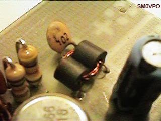
L4 comprises 6 turns of 0.15mm Dia. enamelled wire (magnet wire in the US) wound on TWO ferrite beads, the same beads that were used for L2. The beads are placed side-by-side as a pair of biniculars. One complete turn is when the wire is threaded once though both beads.
L5 is 5 turns of 0.8mm Dia. enamelled copper wire with a 6mm inside diameter. Just as L3, wind it on a drill bit to get the inside diameter correct. The coil is also close-wound. Form the ends of the coil, bending them out then down so that the leads are 5mm apart.
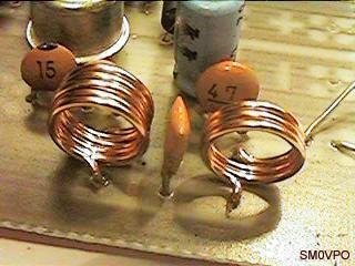
L6 is 3 turns of 0.8mm Dia. enamelled copper wire with a 6mm inside diameter. Just as L3 and L5 the coil is also close-wound. Form the ends of the coil, bending them out then down so that the leads are 5mm apart. You can get a closer view of L5 and L6 in this picture. The position of the capacitor between them is very important, equal distance from both coils keeps the 2nd harmonic at the lowest level.
NOTE - L5 and L6 MUST be wound in the same direction. If you try to wind one of them backwards or in the other direction then the spurious outputs will increase.
The transmitter is constructed on a single-sided printed circuit board. I will place the PCB foil pattern on my DOWNLOAD section of the homepages. The board is only 40mm x 72mm. If you use any other construction method then you will need to change a few component values. If you use veroboard, prototype board then the project will probably not work. The board has been designed to compensate for the lack of a second copper ground land and has also "thermal breaks" around some of the component connections. This makes it easier to solder for new beginners (for me too, but I should not admit that!). I will shortly add a "broadcast" version that does not need any PCB additions for use as a broadcast transmitter. 2x AF inputs, even a prescaler chip on the board!
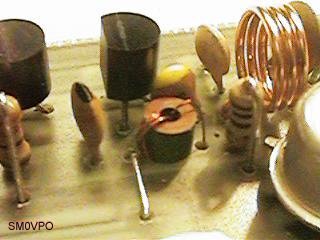
There are two wire links on the board, fit these first. I try to make my links and components as neat as possible with as short leads as possible. Look at the photograph of the finished transmitter to see how they lay. Form the leads and use a bit of masking tape to hold them in position when soldering. The link wires are made using off-cuts from the resistors.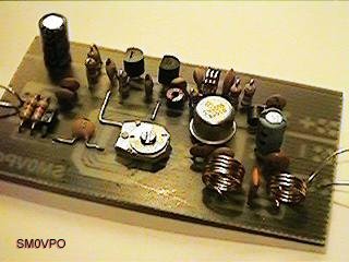
You will note that the 15pf capacitor coupling L1 to the BB105 varicap diode is laying on the board. It´s legs are so formed that it acts as a link. Assembly order is not particularly important, but it is easier if all horisontal components are mounted first, then the passive components (resistors/caps), transistors and the coils last. Neatness and attention to detail is particularly important. The vertically mounted resistors should all be mounted as shown on the component overlay. It DOES matter which way round they are. This is one of the prices for using a cheap single-sided board.
When all the components have been fitted, check your work thoroughly. I reccomend you shine a strong lamp behind the board component side and compare the tracks with the PCB foil pattern. This will allow you to check for solder bridges between tracks. Assuming all is well, connect a 50-Ohm resistor to the antenna (ANT) terminals. Two 100-Ohms in parallel will be fine. Now connect the board to a 9v supply in series with a 12v 3W torch lamp. If the lamp glows brightly then switch OFF and check your wiring because you have a fault. If there is no fault then the lamp should only glow dimly, if it glows at all. The complete transmitter should draw less than 100mA.
If all is well, switch ON an FM radio set tuned to somewhere around 108MHz. Adjust the tuning capacitor on the board so the plates are at around minimum capacitance and you will hear the transmitter on the radio. With the capacitor plates near maximum capacitance you should be able to tune the transmitter to 88MHz.
Now couple the AF IN terminals of the transmitter to the LINE OUT of a stereo ststem, your computer, or even the headphone terminals of your Sony Walkman. I prefer to use headphine terminals since the volume control will give you some control over the modulation depth. You can set the modulation depth by comparing it with another radio channel. Set your transmitter A LITTLE LOWER IN VOLUME than other channels, unless you have access to a modulation meter. Note that you may have to use a capacitor in series with the AF input wire. See the application data further down.
If your transmitter is working then you can remove the test lamp and connect the battery supply directly to the transmitter. Check that nothing is burning. TR3 should get a little warm, but comfortable to the touch. All other components should remain stone cold. TR3 may get a little warmer if you increase the supply voltage to 13.8v but in this case the transmitter will be delivering almost half a watt of output power.
I think that here I should give a little information about the actual measured values of the prototype. The target was to achiece a clean 100mW of output power at 9v. I also indended the transmitter to be equally stable at 13.8v DC since this is what most constructors seem to want. The target was exceeded on all counts. There are no spurious outputs visible from 500MHz upwards, so this spectrum analyser view is only from DC to 500MHz. It shows that there is a little 2nd and 3rd harmonic outputs, but the levels are so low that they are quite negligible. I could hardly believe my eyes when I built the first prototype, but after cleaning up the PCB the output was even better! The vertical scale is 10dB per division and the horisontal scale is 50MHz per division:
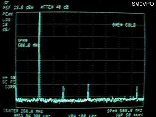
As you can see, the worst case is the 3rd harmonic at -60dBc. The carrier level was +23dBm (200mW) at 10v supply. This falls off a little to about 160mW at the ends of the bands. Brief specifications are given below. I have not been all that meticulous with the figures. When I got a reading of 73mA I rounded it up to 75mA to keep the figures simple. The figures are only a guide anyway.
| Parameter | Supply=9v | Supply=12.5v | Supply=13.8v |
|---|---|---|---|
| Freq range | 76 - 116MHz | 77 - 119MHz | 78 - 121MHz |
| Supply Current (98MHz) | 75mA | 85mA | 95mA |
| Output power (88MHz) | 160mW | 310mW | 370mW |
| Output power (98MHz) | 180mW | 360mW | 420mW |
| Output power (108MHz) | 165mW | 320mW | 380mW |
| Spurious Outputs (DC - 1GHz) | -60dBc | -60dBc | -60dBc |
| RMS AF for +/-75KHz deviation | 210mV | 200mV | 195mV |
| AF response +0/-3dB | 3Hz - 70KHz | 3Hz - 70KHz | 3Hz - 70KHz |
Adjust the variable capacitor to get the transmitter on the frequency you want. Is that simple enough?
There are several different applications since the unit will modulate from DC to several thousand kilohetrz, the most obvious being music. It may be, however, that you wish to change the frequency (to somewhere legal?) and use FSK data for moving information between computers. Perhaps you even want to convey DC changes or just stabilise the TX frequency. Let us now cover these items, beginning with a recap of the circuit diagram:
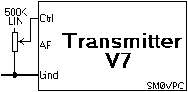
(Not to be used with synthesiser)
As you can see from the original circuit, the varicap voltage is kept high by R1. Without this resistor the DC voltage on the diode will be zero, causing the oscillator to stop. R1 shall be removed if using external synthesiser control. We can, however, use the CTRL terminal to have a preset "frequency" potentiometer on the outside of the box. All we need is a 500K Linear potentiometer. Nothing else! no capacitors, nothing. This will give typically 10MHz tuning range
(Not to be used with synthesiser)
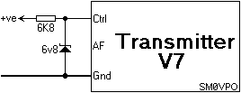
Given that R1 is connected directly to the battery supply voltage, if the battery voltage were to vary then so would the TX frequency. You should really be using a stabilised power supply, or a high-current battery that has a fairly constant supply voltage. If this is NOT the case then you can use the CTRL terminal to bypass R1, without making any modifications to the TX. All we need is an external zener diode and a 6K8 resistor. The Zener diode should be as high as possible. If you have a 12.5v supply, for example, then a 10v diode would be great. With a 9v battery then a 6v8 diode is about the maximum practical. 8v2 would be Ok until the battery voltage went down a bit. We will asume that +VE is a 9v battery.
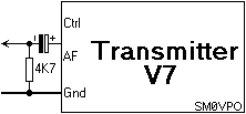
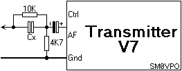
If you are using DC modulation then the AF input will allow this. This can be used to give low frequency Frequency Shift Keying. This should only be done in conjunction with the voltage regulator above. If you are NOT wanting to have a DC shift, and your input source has a "DC Continuity" (resistance) then there is problem. If you were to connect a magnetic microphone or CD player, for example, to the AF input then the TX frequency would jump. You therefore need to add a capacitor to block the DC shift at the input. 10uF will do nicely. A 4K7 resistor should also be added to give a load to the audio source and to help prevent "hum" or "pickup" from 50Hz (60Hz) wiring. The value of the resistor should be selected to match the audio source impedance of the device. 4K7 is normal for computer and CD LINE-OUT signals.
If you wished to use audio directly from a PC or CD-Player, then you should add some form of pre-emphasis. If you are using a stereo encoder or FSK applications then you should NOT use pre-emphasis. Pre-emphasis increases treble a little so that when it is received and turned down again, added noise is also turned down. Select Cx(nf) to be 10x the number of Microseconds of pre-emphasis you want. If you wanted 50uS pre-emphasis then Cx = 50 x 10 nf = 500nf.
The resistor R1 may be removed from the circuit and the loop voltage from a synthesiser added to "Ctrl" on the circuit board. This will give the synthesiser a 10MHz tuning range, the preset capacitor determining the centre frequency. The loop frequency control voltage can be increased to about 20v but it should be maintained somewhere around 9v to get repeatable modulation characteristics.
The coil of the tuned circuit can be reduced and TR1/TR2 replaced for more suitable RF devices, then the TX can be increased to the 144MHz band and modulated with NBFM. In this situation one MUST use synthesiser control to stabilise the frequency.
The transmitter is clean enough to drive larger power amplifiers to get much higher powers. I will be working on both 5-Watts and 25-Watts amplifiers at some time in the future, but exactly when is another question. The more e-mail I get then the longer it will take. My work will be primarily for the 144-146MHz amateur radio band.
I hope that you learn a lot from this project. It demonstrates Varicap diode tuning, decoupling and control. It also shows how to amplify low level signals from the 10mW level to the 150mW level and how DC bias can be applied to make compensations for low signal levels. Have fun with the project. If you have any questions then please do NOT e-mail me. I have a message board where you may post questions to many, some of whom have far more experience than I.
Finally, is there any interest in my producing a kit for this project? I would include the input cap, pre-emphasis and Zener on the kit PCB, but there would be details showing how to bypass this for those who wish to do more than just send music. Please let me know at harryvpo@hotmail.com keeping your mail short as possible, thanks.
Very best regards from Harry - SM0VPO, Lunda, Sweden.