
This version will operate from 9v DC to 36vDC but you much choose a transformer to suit the supply voltage. It does not (yet) have any voltage regulation. The output waveform is (almost) identical to the 02 version but there is a slight gap between the +ve and -ve pulses. The frequency of this version can be selected for 50Hz or 60Hz. The output power of my prototype is 250 Watts but I have pushed it to 350 Watts. So to recap, the features of this project are:
Inverter options are:
| Input Voltage | Qty IRF510 | Output power | Transformer | Current rating |
|---|---|---|---|---|
| 9v | 2 | 30 | 9-0-9v - 115 / 230v | 6 Amps |
| 9v | 4 | 60 | 9-0-9v - 115 / 230v | 12 Amps |
| 12v | 2 | 60 | 12-0-12v - 115 / 230v | 6 Amps |
| 12v | 4 | 120 | 12-0-12v - 115 / 230v | 12 Amps |
| 18v | 2 | 90 | 18-0-18v - 115 / 230v | 6 Amps |
| 18v | 4 | 180 | 18-0-18v - 115 / 230v | 12 Amps |
| 24v | 2 | 120 | 24-0-24v - 115 / 230v | 6 Amps |
| 24v | 4 | 240 | 24-0-24v - 115 / 230v | 12 Amps |
| 36v | 2 | 180 | 36-0-36v - 115 / 230v | 6 Amps |
| 36v | 4 | 360 | 36-0-36v - 115 / 230v | 12 Amps |
The circuit is almost identical to the 02 version and is divided into two part:
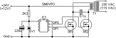
Beginning with the voltage regulator, this is a 2K2 (2200 Ohms) resistor fed from the DC input, which drives an operating current through a 5.1 Volt Zener diode. A 220uf electrolytic capacitor is connected across the diode to remove any power supply glitches, spikes or Zener noise that may otherwise exist. A further capacitor and LED are added in the processor -ve ground path. This effectively raises the processor ground supply voltage to give a logic-level shift of 5 volts with 1.5v added. The 5v logic levels from the processor to the power FETs is therefore +1.5v = logic "0" (low) and +6.5v = logic "1" (high). This places the logic levels from the processor in the middle of the FET operating characteristics. The FETs will always be turned hard ON, which means they will not dissipate any power.
The 5.1 Volt regulator must be tested before the processor chip is plugged into the circuit, otherwise a wiring error could prove costly (US$2.5). The LED must also glow a little. It will be quite weak at 9v but if using +36v supply it may be quite bright. Note that the LED is a normal "bog standard" good-old ordinary RED LED.
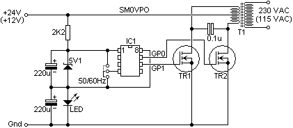
The processor GP0 (pin 7) and GP1 (pin 6) are connected to the Gates of the two IRF510 power FETs. The Source terminals of the FETs are grounded and the Drain terminals are connected to the transformer. The processor pin 4 (GP3) is programmed as an input port to sense the 50/60Hz link. According to the processor specifications there is a weak pull-up resistor connected to this pin, but in this application there is an awfull lot of EMF and magnetic pulses floating around, so I have made the link a 2-position link.
The microprocessor does everything and uses the internal 4 MHz oscillator so no other external components are needed. The IRF510 will be switched hard-ON or hard-OFF by the 5 Volts square-wave (+1.5v to +6.5v) from the processor, so no voltage level or current buffering is needed. The transistors are fed directly.
An additional 0.1uF non-electrolytic capacitor is fitted to the board to stop any tendency to ringing, but since either TR1 or TR2 is always low-impedance the transformer is always well damped anyway. This component should be rated at twice the input voltage, plus a bit extra. For example, if you have 36v input then the actual peak DC level from lead-acid accumulators can be 2.4166 volts per cell. 18 cells (36v nominal) can be as high as 43.5v. Use a 60v non-electrolytic capacitor.
The transformer can be a 230v (or 115v) to 12v-0v-12v type capable of handling 5 Amperes. This means a 60 Watt transformer. If you choose a torroidal type then the no-load standing current can be lower than 50mA :-) You can alternatively choose a 230v (or 115v) to 24v-0v-24v transformer and get 120 Watts output. No other components need be changed at all. I gave this circuit a brief trial at 36vDC input using three car batteries. Unfortunately I only had a 24v transformer so I did not test it for very long. But I did get a nice solid 350vAC out.
To give you a few examples of power, transistors and transformer options here are a few variants:
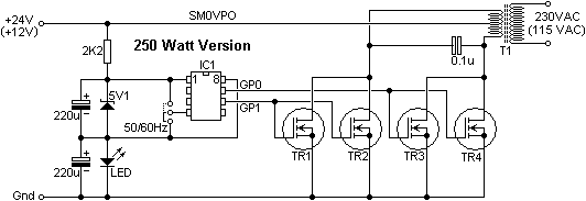
This version with four transistors is the maximum one single PCB will take. This represents 250 Watts at 24V DC in or 125 Watts at 12V DC in. Of course you can add more external transistors and transformers to get a lot more power out. Here's how you do it:
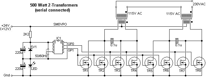
Note that you MUST be aware of the transformer secondary winding phase: the two transformers should be connected identcally. If you are unsure then connect them in SERIES and check that you get double the voltage you want. If the phases are wrong then you will get no voltage at all.
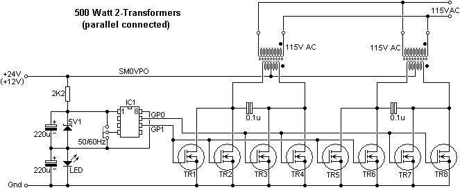
Note that you MUST be aware of the transformer secondary winding phase: the two transformers should be connected identcally. If you are unsure then connect them in SERIES and check that you get double the voltage you want. If the phases are wrong then you will get loads of sparks, sizzling noises and heaps of smoke. The neighbours will smell the acrid smoke and call the fire brigade. The police will want to know what the heck you have been doing, and I absolutely refuse to take any blame whatsoever. It is YOUR arse on the line so you don't want anyone sniffing around.
The transformer options are endless. There is absolutely no reason why you cannot extend this to 1000 Watts or more. Just don't get silly with the expansion. 100,000 Watts is probably a bit too much without a couple of BC547s to buffer the processor ;-)
The printed circuit board is given in the download section of these homepages. The large lands of copper were deliberately chosen to act as a heat-sink, as well as handle 12 Amperes. I ran the prototype for about an hour at 200 Watts continuous and the FETs remained stone-cold. The transistors are simply bolted to the boards without any of those insulation mica washers: just a pair of good-old M3 (or 6BA) bolts. Put two nuts on them and you can use the bolts as terminals for the transformer. All component holes are 0.9mm Diameter, except for the power tags of the transistors, which are 3mm Diameter. I also used a 3mm Diameter hols for the power GND connection. I would reccommend you use a washer between the bolt head and the PCB track to get a good connection. The current in the board can be as high as 12 Amperes. I did a few experiments using three 60W car lamps at 12v and the 15 Amperes did not cause any noticeable heating of the board if the bolts are nice and tight.
Note that the resistor I used was 2K2 for both 12 and 24 Volts input. 2K2 provides the 10mA - 15mA peaks the 12F509 (IC1) requires. Without loads it only needs a few hundred micro-amperes but the capacitive load of the FETs can theoretically require more current. I calculated over 10mA for eight power FETs, but the capacitor across the zener should provide this current without any problem.
Although I have called this a prototype, I believe it to be finished. There will be no further hardware development on this board. There may be software development but if any hardware changes, other than unforseen corrections, then there will be a new project. This particular project functions perfectly, stone-cold and has been feeding a 42" flat-screen television. So here are the photographs:
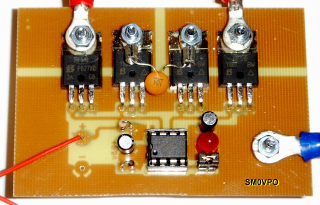
As you can see it is identical to the component overlay with no corrections or modifications. This version has four transistors and delivers over 200 Watts.
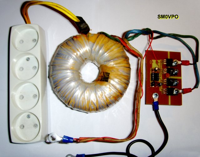
This particular transformer I used came from the Swedish Royal technical High-School technical rubbish skip. I normally check the skip daily as there are loads of interesting goodies there. The transformer is 230v to 18v-0v-18v at 12 Amperes. This gives me a nice 225 Watts continuous. This circuit was running continuously for 60 minutes with a towel over it to restrict heat dissipation. It never even got warmer than body temperature! When not covered it was stone-cold.
You can easily extend the board by adding extra transistors to give you 24, 36 Amperes or more input current. At 24v input his equates to 500 Watts or 1000 Watts output. I will not be expanding the board at all. If you want to expand it yourself then use a second board and connect the two processor inputs to the main board.
Power transformers are rather hard to get hold of, so there is no reason why you cannot use more than one transistor in parallel. As long as the transformers are identical in every way, there is no problem. You could use two 24-0-24v @ 12A to 115v transformers. Connect the two 24v secondary windings to two sets of power transistors and then you can connect the 115v windings in parallel for 115V or series for 230V AC out.
Whi not use four transformers in series/parallel connection?
One small word of warning: I would strongly suggest the DC input and AC outputs be fused. If you overload this inverter then unlike many other designs it will simply NOT sag or sink. The transistors will still push out power according to your demand, and do so until the output devices literally explode. Another BIG word of warning: the output of this unit can kill. Electrical shocks can be fatal. If you have no clue as to what you are doing, or if you have never used high-voltage circuits before then do not attempt this project. It is YOUR arse on the line so you don't want a cockup.
Ok, like the MkII, this Mk III project also uses software. Guilty once more!! If you have a PIC programmer then you can download the HEX file and burn it yourself using PICProg4U or WINPROG. I am using the MPLabs PIC-Kit2 assembler and the RCD programmer. This nice little programmer is published by Feng3, which you can download and use for free. The HEX file you need is pic-inverter_03_code.hex, which you download and burn to the processor flash memory. Right-click the link and save the file to your hard disk.
If you wish to modify the code for your own application then you will need the source code. If you want a chip ready programmed then you can send me US$2.50 per chip and US$4.50 to cover postage (any reasonable quantity). For one chip this is US$7 (SEK50) including postage.
If you want the chips for commercial use then please call me: If you are going to make a profit from my work then I would like US$1.50 commission per chip. Here is my ASM file:
;************************************************************************
;   Filename:      50hz generator                                       *
;   Date:          2012-04-19                                           *
;   File Version:  2.0                                                  *
;                                                                       *
;   Author:        Harry Lythall, SM0VPO                                *
;************************************************************************
;   Architecture:  Baseline PIC                                         *
;   Processor:     12F508/509                                           *
;************************************************************************
;   Files required: none                                                *
;************************************************************************
;   Description:    DC/AC generator, single phase                       *
;                                                                       *
;   Toggles GP0 and GP1 at 50Hz (60Hz) anti-phase                       *
;   25uS delay between GP0=ON and GP1=ON                                *
;   GP1 and GP2 drive push-pull power MOSFETS.                                     *
;                                                                       *
;************************************************************************
;   Pin assignments:                                                    *
;       GP0 (pin7) - out - Toggling                                     *
;       GP1 (pin6) - out - Toggling in oposition to GP1                 *
;       GP3 (pin4) - in  - select 1=50Hz 0=60Hz (1=50Hz)                *
;                                                                       *
;************************************************************************

    list        p=12F509
    #include

                ; ext reset, no code protect, no watchdog, 4Mhz int clock
    __CONFIG    _MCLRE_OFF & _CP_ON & _WDT_OFF & _IntRC_OSC


;***** VARIABLE DEFINITIONS & SETUP
        UDATA
dc1     res 1                   ; delay loop counters
dc2     res 1

RESET   CODE    0x000		; effective reset vector
        movwf   OSCCAL		; update OSCCAL with factory cal value

start	movlw   b'111100'	; configure GP0 + GP1 as outputs
        tris    GPIO


;**************************** Inter-pulse delay
Main	call	Del4

;**************************** Switch GP0=ON GP1=OFF
	movlw	b'000001'	; set w to 1 in bit0
	movwf	GPIO		; set GP0 high - GP1 low


;**************************** Test 50/60 select and wait
	btfsc	GPIO,3		; Test GP3 - skip next if 0
	call	Del5		; GOSUB for 20mS
	btfss	GPIO,3		; Test GP3 - skip next if 1
	call	Del6		; GOSUB for 17mS

;**************************** Inter-pulse delay
	call	Del4

;**************************** Switch GP0=OFF GP1=ON
	movlw	b'000010'	; set w to 1 in bit0
	movwf	GPIO		; set GP0 high - GP1 low

;**************************** Test 50/60 select and wait
	btfsc	GPIO,3		; Test GP3 - skip next if 0
	call	Del5		; GOSUB for 20mS
	btfss	GPIO,3		; Test GP3 - skip next if 1
	call	Del6		; GOSUB for 17mS

;**************************** Finished, now do it again
	goto	Main


; SUBROUTINES:
;**************************** Switch off ports for 25uS
Del4	movlw	b'000000'	; set w to all zero
	movwf	GPIO		; write to GP0 + GP1
	movlw	.10
	movwf	dc1
Del4a	decfsz	dc1
	goto	Del4a
	retlw	0

;**************************** Delay loop for 50Hz
Del5	movlw	.232		; 200 x 50uS
	movwf	dc1
Del5a	movlw	.13		; 50uS
	movwf	dc2
Del5b	decfsz	dc2
	goto	Del5b		; not 50uS yet
	decfsz	dc1		; another 50uS ?
	goto	Del5a		; yes
	retlw	0		; Done

;**************************** Delay loop for 60Hz
Del6	movlw	.192		; 192 x 50uS
	movwf	dc1
Del6a	movlw	.13		; 50uS
	movwf	dc2
Del6b	decfsz	dc2
	goto	Del6b		; not 50uS yet
	decfsz	dc1		; another 50uS ?
	goto	Del6a		; yes
	retlw	0		; Done

        END
I used MicroChip's MPLab to assemble the program. The first section of the program is needed to define the starting parameters of the process. This means defining the two output ports and the input port. It also selects the internal 4MHz clock oscillator. Each chip is factory programmed with a calibration value and this value is alread and used to calibrate the chip.
The MAIN routine does four things:
When these four steps are completed the GOTO MAIN starts it all over again.
Since the 50/60Hz select input is sensed every cycle it is theoretically possible to change in operation, but this means stuffing grubby fingers charged with static electricity in to the circuit. If you have a switch on the front panel then this is a possibility, but otherwise forget it.
The "Del5" and "Del6"rountines have a delay of 10mS or 8.33mS, which is the delay needed for either 50Hz or 60Hz half-cycles. The output port status is changed and the delay loops are called again. The values 232 (50Hz) or 192 (60Hz) can be adjusted for individual processor chips to give a more precise frequency output, but this varies frome one processor to another. In this version I deviated from the Gooligum Electronics (Australia) tutorials and did not bother with the shadow register for output ports. I thought it was a lot simpler to do this.
As a matter of interest, the IRF510 will operate into the VHF region, which means that you can screw the frequency of this little inverter up to a few 10s of kHz for a more efficient converter. If you needed to get 250vDC for a valve (tube) project then this would be ideal and with only a miniature SMPSU ferrite transformer.
Finally, if you re-use these processor chips then it is easy to erase the factory oscillator calibration value. The first two digits are always the same, but the second two digits vary. What you can do is read the value, then take a overhead marker pen and put dots on the legs of the chip, on the flat bit where they enter the package. There are eight pins which can record two HEX digits.
If you have any technical questions then I try to answer all e-mail questions, but it may often take time. I would prefer you used my messageboard for technical queries and discussions. There are many people more clever than me using the board.
No. I now have a new "bionic eye" so I can make PCBs, but unfortunately my priorities and Maj-Lis's priorities are somewhat different. As a result I do not have much time for for making PCBs at this moment in time. Spring is here and that means spending time renovating the house and doing a bit of garden work. Sorry!!
These projects are all 100% free for non-profit private use. You may download and use all my projects, PCB foil patterns and software for prive use. These projects have taken years to create and are free from membership fees, advertising and banners.
If you wish to donate to HHH then donations are always appreciated to harry.lythall(at)sm0vpo(dot)com via www.paypal.com.
Best regards from Harry - SM0VPO
Return to INFO page